12. System On Chip
The heterogeneity of computer system is increasing at a fast pace. In the server space, we have long seen the use of dedicated accelerators for higher throughput. Traditionally, these have been GPUs tied to host CPUs. In recent years accelerators other than GPUs have gained popularity in the server space as well. For example, consider Intel’s Knights Corner or Google’s Tensor Processing Units. From a hardware-perspective, these accelerators are realized on different chips and connected to the host-CPU through the motherboard. In the offloading model, compute-intensive task are offloaded to the accelerator whereas the hosting CPU orchestrates the executions and handles data movements between multiple accelerators.
System on Chip (SoC) designs integrate different components into a single integrated circuit. This means that the CPU, internal memory and accelerator(s) are all on the same chip. The integration leads to a tighter coupling, where, for example, the accelerators and CPU can access the same memory. Certain tightly integrated acceleration engines, e.g., Apple’s AMX unit, even use the same instructions stream as the CPU and have access to the CPU’s cache. Currently, SoCs are heavily used for mobile and edge devices. In the smartphone space, prominent examples are Apple’s Bionic line of SoCs, Qualcomm’s Snapdragon platforms and Samsung’s Exynos family. SoCs are also becoming popular in the personal computing space. Examples are Apple’s M1 and M2 SoCs, AMD’s Ryzen 7040 series, or Intel’s Meteor Lake processors. At the moment, the acceleration of workloads in the server space largely relies on dedicated accelerators. However, upcoming computer architectures, such as Nvidia’s Grace Hopper Superchip or AMD’s MI300 APU are already striving for a tighter integration as well.
This lab studies the Snapdragon 8 Gen 2 Mobile Platform which combines a diverse set of computing devices. In detail, we will have a look at the SoC’s Central Processing Unit (CPU) in Section 12.2, at the SoC’s Graphics Processing Unit (GPU) in Section 12.3, and at the compute Digital Signal Processor (cDSP) in Section 12.4.
12.1. Android
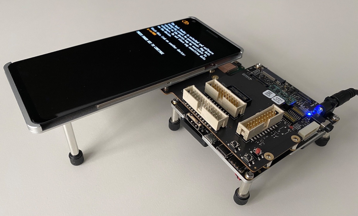
Fig. 12.1.1 Illustration of the HDK8550 Development Kit used in this lab. The main board hosts a SM8550P system on chip.
This lab explores the HDK8550 Development Kit. The development kit consists of a main board which features the SMP8550P SoC, a display card, a camera card and a sensor card. One of the kits is shown in Fig. 12.1.1.
The development kits run the Android operating system in version 13. Thus, before diving into the details of the SoC, we’ll get used to the Android operating system and the corresponding Android toolchain. In comparison to previous labs, we’ll use the same user to log into the kits. This means that you share the devices and the user accounts with your fellow students.
Important
Create your own directory in
/data/local/tmp/. Use your first name for the name of that directory. Do not touch files anywhere else on the file system!The development kits have enabled root access. Run root commands only if explicitly instructed to do so!
Coordinate with your peers when using the devices. Use the class’s matrix channel for this when not in the lab room.
The kits are connected to a server which you can reach under soc.inf-ra.uni-jena.de when in the university’s network.
Login details are discussed in class.
Tasks
Use the Android Debug Bridge (adb) to push a text file to your directory in
/data/local/tmp. Open an adb shell and print the contents of your file.Cross compile a simple C++ program for the Kryo CPU which prints “Hello World!”. Transfer the executable to the device and run it on the device.
Use
adb logcatto monitor the device. Ask a peer to power on the display while you are monitoring the device. You may power on the display by pressing the push button labeled “PON”.
12.2. CPU
The SM8550P SoC has an Armv9-based Qualcomm Kryo CPU which is by itself heterogenous. Specifically, the CPU comprises one prime core with a frequency of up to 3.2 GHz, four performance cores (up to 2.8 GHz) and three efficiency cores (up to 2.0 GHz). The prime core uses Arm’s Cortex-X3 microarchitecture. Two of the performance cores use the Cortex-A715 microarchitecture while the other two use the Cortex-A710 microarchitecture. The three efficiency cores are based on Cortex-A510.
This high degree of heterogeneity is different from what we have seen until now. For example, the cores of Graviton3 are all identical, i.e., we obtain the same performance no matter which of the Graviton3 cores execute our workload. In this part of the lab we will study the heterogeneity of Kryo CPU by testing our ASIMD microkernels and small matrix multiplication kernels. Thus, from a software standpoint, we program the CPU using Arm Assembly called from our usual C/C++ drivers.
Note
Due to the installed Android operating system, we may only execute ASIMD workloads and not our SVE code.
We use taskset to control which cores execute our workload. The pinning procedure is a bit cumbersome, there’s a free coffee in it for you if you find a simpler approach:
Open two connections to the development kit using
adb shell. We use the first shell to execute our benchmarks and the second to pin the respective process.In the executing shell:
Launch the program of interest and get the process id of the running program.
You may print the program id programmatically through the getpid() function.
In the pinning shell, use
taskset -p MASK PIDto pin the process to cores:Provide the the desired mask as
MASKin the taskset command. The command expects a hexadecimal number which encodes the desired pinning. For example,taskset -p 80would pin the process to the eighth core since \(80_{16} = 10000000_2\). Similarlytaskset -p 48would use the fourth and the seventh core since \(48_{16}=01001000_2\).Use the process id of the launched program as
PIDin the command above.You may confirm the pinning by studying the two lines
Cpus_allowedandCpus_allowed_listin/proc/PID/status.
The program which is being pinned has to run for this procedure to work. Attempts to do the pinning at program startup or when waiting for user input in the program have failed so far (☕?).
Tasks
Test the Snapdragon Profiler to monitor the utilization of the SoC.
Benchmark the Kryo CPU using your ASIMD microkernels (developed in Section 1). Identify ids of the cores which are associated with the CPU’s prime core, the performance cores and the efficiency cores. Report the obtained FP32 and FP64 performance for all cores.
Run your ASIMD matrix kernels, developed in Section 6.2 on the X2 core. Report the obtained performance.
12.3. GPU
This part has a look at the Adreno 740 GPU of the SM8550P SoC. From a developer’s perspective we may program the GPU using then Open Computing Language (OpenCL). OpenCL is cross-platform standard for programming heterogenous processors. An OpenCL application is portable, i.e., it may run on different accelerators if no vendor-specific extensions are used. For example, we could execute the same application on a CPU or the SoC’s Adreno GPU. However, program portability does not imply performance portability. This means that while an OpenCL application may run on diverse accelerators, additional device-specific tuning is required to exploit the hardware efficiently. Qualcomm provides the Snapdragon Mobile Platform OpenCL General Programming and Optimization Guide which provides respective details for Adreno GPUs.
Hint
The course Hands On OpenCL provides a more gentle introduction into OpenCL.
We’ll perform three steps to explore OpenCL and Adreno GPUs: First, we code a simple device query which discovers available devices and shares device information through the OpenCL platform layer. Second, we implement our standard triad example, i.e., \(c[:]=a[:]+2 \cdot b[:]\), using OpenCL. We’ll do this at first by copying the three arrays from host to device memory, then executing an OpenCL triad kernel, and copying the data back from device memory to host memory. This is the “traditional” offloading approach for programming GPUs where one explicitly handles the host-device data transfers. Additionally, we’ll have a look at an advanced version which avoids the host-device memory copies by using mmap on DMA buffers. This allows us to share memory between device and host. Last, we’ll implement a matrix-matrix multiplication which executes on the Adreno GPU. As part of this effort we’ll learn about vector operations in OpenCl. Examples are vload4 or vstore4.
Tasks
Implement a device query program using OpenCL. Print information about the platform using clGetPlatformInfo (including
CL_PLATFORM_VERSIONand theCL_PLATFORM_NAME). Obtain important device information using clGetDeviceInfo. Include at leastCL_DEVICE_NAME,CL_DEVICE_OPENCL_C_VERSION,CL_DEVICE_MAX_COMPUTE_UNITS,CL_DEVICE_LOCAL_MEM_SIZEandCL_DEVICE_GLOBAL_MEM_SIZEin your print statements.Implement an OpenCL kernels which executes the triad \(c[:]=a[:]+2 \cdot b[:]\) on device. Initialize the arrays on the host and use clEnqueueWriteBuffer to copy data from the host to the device, and clEnqueueReadBuffer to copy data from the device to the host. Use the following function signature for your kernel:
__kernel void triad( __global float * i_a,
                     __global float * i_b,
                     __global float * io_c )
Revisit your triad code and implement a zero-copy version. Follow the approach of function
dmabuf_buffer()in thesrc/examples/dmabuf_buffer_and_image/dmabuf_buffer_and_image.cppexample of the Qualcomm OpenCL SDK.Implement the FP32 matrix-matrix multiplication C+=AB in OpenCL. Use a 4 by 8 blocking for matrix C and float4 vector data types for the values of A and C.
12.4. cDSP
The Hexagon Processor will be our last targeted accelerator of the Snapdragon Platform. While the entire chip comprises multiple Digital Signal Processors (DSPs), we’ll exclusively study the compute DSP (cDSP). The cDSP of the SM8550P SoC supports base instructions, the Hexagon Vector eXtension (HVX) and the Hexagon Matrix eXtension (HMX). Since HMX instructions are not publicly documented, the HMX unit is only accessible through Qualcomm tools, e.g., the Qualcomm Neural Processing SDK. Thus, we’ll rely on HVX instructions to drive the performance of our kernels.
From a programmer’s perspective the DSP is used through Remote Procedure Calls (RPCs).
This means, that a program running on the host CPU uses the FastRPC framework to call functions on the DSP device.
We’ll largely ignore the RPC part of the DSP and use a prepared code frame which takes care of the host-device communication for us.
Instead we’ll focus on writing high-performance matrix kernels using HVX assembly and on the threading capabilities of the Qualcomm Hexagon Real-Time operating system (QuRT).
Hint
The Hexagon SDK provides extensive documentation, hints and examples on the efficient utilization of the available DSPs.
You may install a recent version of the SDK using the Qualcomm Package Manager.
A recent version is also available on the server soc.inf-ra.uni-jena.de hosting the development kits.
The documentation is available from the directory /opt/HexagonSDK/5.3.0.0/docs/.
Writing efficient assembly code for the cDSP is fundamentally different to what we have done for out-of-order Arm processors so far. When writing small matrix-matrix multiplication kernels, we have to be aware of at least the following differences:
The DSP uses a Very Long Instruction Word (VLIW) instruction set architecture. This means, that we have to group up to four instructions into packets which are then executed in parallel.
The cDSP microarchitecture is in-order, i.e., the hardware won’t reorder our instruction packages and simply stall in the case of occurring dependencies.
The HVX coprocessor may perform 128-byte vector instructions.
HVX uses a custom floating point format (qfloat) which deviates from the IEEE-754 standard.
The DSP offers hardware loops.
Tasks
Implement a microkernel which assesses the maximum attainable qfloat32 performance. Use
vmpyandvaddinstructions in your kernel. Name your kernelmicro_hvx_qf32and call it using a single QuRT thread.Extend the previous benchmarking effort by calling
micro_hvx_qf32from multiple QuRT threads. What is the maximum attainable qfloat32 performance of the entire cDSP?Implement the unrolled matrix kernel C += AB for M=192, N=4, K=1, ldA=192, ldB=1, ldC=192. Use the following function signature for your kernel:
void gemm_asm_cdsp_192_4_1( float const * i_a,
                            float const * i_b,
                            float       * io_c );
Submit the metrics “time (s)”, “#executions”, “GFLOPS” and “%peak”.
Implement the matrix kernel C += AB for M=192, N=4, K=128, ldA=192, ldB=128, ldC=192. Use the following function signature for your kernel:
void gemm_asm_cdsp_192_4_128( float const * i_a,
                              float const * i_b,
                              float       * io_c );
Submit the metrics “time (s)”, “#executions”, “GFLOPS” and “%peak”.