5. Arithmetic Logic Unit
This lab implements an Arithmetic Logic Unit (ALU).
ALUs are the computational heart of most processors.
As shown in Table 5.1, our ALU supports the operations add, sub, and, and or.
We can choose the ALU’s desired functionality through a two-bit control signal.
Control Signal |
Operation |
|---|---|
2’b00 |
add |
2’b01 |
sub |
2’b10 |
and |
2’b11 |
or |
In Section 5.1 we first design the ALU pieces required for the operations in Table 5.1. Once the supporting pieces are in place and tested, we implement a basic ALU. Section 5.2 tasks will bring our design to the DE10-Lite board and allow us to control the ALU through the board’s slide switches. We’ll then extend our initial ALU by adding condition flags in Section 5.3. As discussed further in Section 5.4, the condition flags allow us to interpret the results of our operations. Lastly, Section 5.5 deploys the extended ALU to the DE10-Lite board.
Hint
Respective schematics of the basic 64-bit ALU and extended ALU are provided throughout this lab. These are sufficient to solve the tasks. In addition, an interactive and very similar implementation of the 4-bit parts is available on CircuitVerse
5.1. Designing a Basic ALU

Fig. 5.1.1 Illustration of our ALU’s basic part for 64-bit inputs i_a and i_b, and the 2-bit control signal i_alu_ctrl.
This section designs the initial part of our ALU which is shown in Fig. 5.1.1.
The two N-bit values i_a and i_b, and the control signal i_alu_ctrl represent the inputs to our basic ALU.
Outputs are given through the N-bit value o_result and the carry-out o_carry_out.
Building Blocks
We identify three submodules, which we’ll design with the following declarations before tackling the entire ALU:
An N-bit adder.
module adder #(parameter N=64) ( input  logic [N-1:0] i_a,
                                                      i_b,
                                 input  logic         i_carry_in,
                                 output logic [N-1:0] o_s,
                                 output logic         o_carry_out );
A 2:1 multiplexer which is used as an input to the N-bit adder.
module mux_2 #(parameter N=64) ( input  logic [N-1:0] i_in0,
                                                      i_in1,
                                 input  logic         i_s,
                                 output logic [N-1:0] o_out );
A 4:1 multiplexer which is used to select the final result.
module mux_4 #(parameter N=64) ( input  logic [N-1:0] i_in0,
                                                      i_in1,
                                                      i_in2,
                                                      i_in3,
                                 input  logic [1:0]   i_s,
                                 output logic [N-1:0] o_out );
Tasks
Implement the module
adderin the fileadder.sv. Test your implementation in the testbenchadder_tbin the fileadder_tb.sv. Check at least three test cases!Implement the module
mux_2in the filemux_2.sv. Test your implementation in the testbenchmux_2_tbin the filemux_2_tb.sv. Check at least three test cases!Implement the module
mux_4in the filemux_4.sv. Use the previously implemented modulemux_2in your implementation ofmux_4! Test your implementation in the testbenchmux_4_tbin the filemux_4_tb.sv. Check at least three test cases!
Putting the Parts Together
We have all building blocks at hand to implement the basic version of our ALU. We’ll use the following SystemVerilog declaration (see also Fig. 5.1.1):
module alu #(parameter N=64) ( input  logic [N-1:0] i_a,
                                                    i_b,
                               input  logic [1:0]   i_alu_ctrl,
                               output logic [N-1:0] o_result,
                               output logic         o_carry_out );
Before going into the details of the design, let’s derive some example inputs and outputs. These also build the minimum example values for our ALU’s testbench.
i_a |
i_b |
i_alu_ctrl |
o_result |
o_carry_out |
|---|---|---|---|---|
8’b0000_0000 |
8’b0000_0000 |
2’b00 |
8’b0000_0000 |
1’b0 |
8’b1011_1101 |
8’b1010_0101 |
2’b00 |
8’b0110_0010 |
1’b1 |
8’b1011_1101 |
8’b1010_0101 |
2’b01 |
||
8’b1011_1101 |
8’b1010_0101 |
2’b10 |
||
8’b1011_1101 |
8’b1010_0101 |
2’b11 |
Tasks
Fill in the missing parts of Table 5.1.1.
Implement the module
aluin the filealu.sv. Test your implementation in the testbenchalu_tbin the filealu_tb.sv. Add respective tests for all examples in Table 5.1.1 toalu_tb.Generate a waveform plot illustrating the application of your ALU w.r.t. Table 5.1.1’s inputs. Limit your plot to these inputs and change the input every 10 time units, i.e., visualize 50 time units. The plot shall show all inputs, i.e.,
i_a,i_bandi_alu_ctrl, and all outputs, i.e.,o_result,o_carry_out.
5.2. Basic ALU in Practice
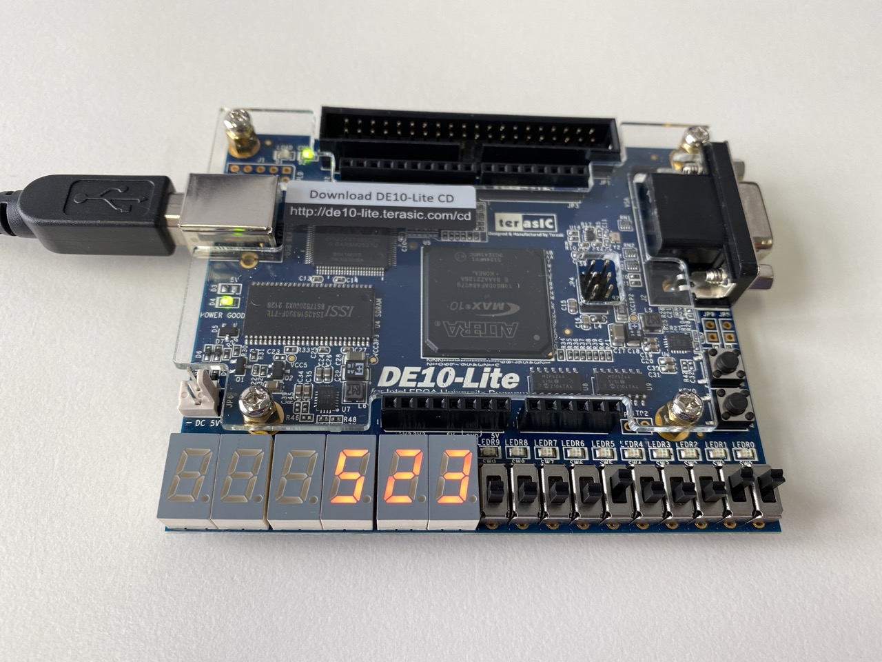
Fig. 5.2.1 Picture of the deployed arithmetic logic unit.
Shown is the configuration for inputs i_a[3:0]=4'b0011, i_b[3:0]=4'b0010 and i_alu_ctrl[1:0]=2'b00.
Our design is finished and the simulations look promising: Lets put the ALU into production!
An example configuration of a deployed design is shown in Fig. 5.2.1.
For this we write a top-level module alu_de10_lite for the DE10-Lite board.
The module instantiates a 4-bit version of our module alu and maps the board’s switches to the inputs i_a[3:0], i_b[3:0] and i_alu_ctrl[1:0].
Specifically, we wire SW[3:0] to i_a[3:0], SW[7:4] to i_b[3:0], and SW[9:8] to i_alu_ctrl[1:0].
As done for the tiny calculator in Section 4.3, we show the input i_a[3:0] on display HEX0 and i_b[3:0] on display HEX1.
The result o_result[3:0] goes to display HEX2.
However, we use a different strategy for the control signal i_alu_ctrl[1:0] and the carry-out signal o_carry_out.
We show the first bit of the control signal, i.e., i_alu_ctrl[0:0], by activating LEDR0 if the signal is 1, and the second one, i.e., i_alu_ctrl[1:1], through LEDR1.
Further, we indicate a non-zero carry-out signal by wiring o_carry_out to LEDR7.
i_a |
i_b |
i_alu_ctrl |
o_result |
o_carry_out |
|---|---|---|---|---|
4’b0011 |
4’b0010 |
2’b00 |
4’b0101 |
1’b0 |
4’b1011 |
4’b1010 |
2’b01 |
4’b0001 |
1’b1 |
4’b1001 |
4’b1110 |
2’b10 |
4’b1000 |
1’b1 |
4’b1001 |
4’b1110 |
2’b11 |
4’b1111 |
1’b0 |
 1/**
 2 * Top-level module of the basic alu.
 3 * The alu operates on the 4-bit binary numbers in SW[3:0] and SW[7:4].
 4 * The two input numbers are shown on displays HEX0 and HEX1.
 5 * The control signal is shown using LEDR1 and LEDR0.
 6 * The result is shown on display HEX2.
 7 * The carry out is shown via LEDR7.
 8 *
 9 * @param SW bits of ten switch buttons SW9 - SW0.
10 * @param LEDR output bits corresponding to the board's ten leds LEDR9 - LEDR0.
11 * @param HEX0 output bits which drive the seven-segment display HEX0.
12 * @param HEX1 output bits which drive the seven-segment display HEX1.
13 * @param HEX2 output bits which drive the seven-segment display HEX2.
14 **/
15module alu_de10_lite( input  logic [9:0] SW,
16                      output logic [9:0] LEDR,
17                      output logic [6:0] HEX0,
18                      output logic [6:0] HEX1,
19                      output logic [6:0] HEX2 );
20  logic [1:0] l_alu_ctrl;
21  logic [3:0] l_a;
22  logic [3:0] l_b;
23  logic [3:0] l_result;
24  logic       l_carry_out;
25
26  // "rename" inputs
27  assign l_alu_ctrl[1:0] = SW[9:8];
28  assign l_a[3:0] = SW[3:0];
29  assign l_b[3:0] = SW[7:4];
30
31  // alu
32  alu #(4) alu_4( l_a,
33                  l_b,
34                  l_alu_ctrl,
35                  l_result,
36                  l_carry_out );
37
38  // TODO: finish the implementation by wiring the outputs
39
40endmodule
Tasks
Implement the top-level module
alu_de10_lite. Use the template in Listing 5.2.1.Compile your finished ALU in Quartus Prime and program the FPGA of a DE10-Lite board.
Make sure that the boards shows the correct results for the inputs in Table 5.2.1. Provide a picture of the board for each of the inputs.
5.3. NZCV-Extended ALU
Now, let’s extend our ALU by a set of condition flags which provide information about our ALU’s results. Specifically, we’ll introduce the NZCV flags whose meaning is given in Table 5.3.1 These flags are commonly used in practice and a large variety of instructions rely on them. For example, the Arm ISA uses NZCV flags extensively for conditional branching.
Flag |
Meaning |
|---|---|
Negative |
The output of the ALU is negative. |
Zero |
The output of the ALU is zero. |
Carry |
Unsigned overflow on an addition / subtraction. |
oVerflow |
Signed overflow on an addition / subtraction. |
module alu_nzcv #(parameter N=64) ( input  logic [N-1:0] i_a,
                                                         i_b,
                                    input  logic [1:0]   i_alu_ctrl,
                                    output logic [N-1:0] o_result,
                                    output logic [3:0]   o_nzcv );
We implement the NZCV flags by extending our original module shown in Fig. 5.1.1.
The SystemVerilog declaration of the extended design is given in Listing 5.3.1.
Compared to the declaration of our initial ALU given in Listing 5.1.1, the module alu_nzcv does not output the carry-out signal o_carry_out directly anymore.
Instead we output four bits for the NZCV flags in o_nzcv.
We extend the ALU shown in Fig. 5.1.1 by introducing the flags one-by-one:

Fig. 5.3.1 Illustration of our partially extended ALU after adding support for the Zero flag.

Fig. 5.3.2 Illustration of our partially extended ALU after adding support for the Zero and Negative flags.

Fig. 5.3.3 Illustration of our partially extended ALU after adding support for the Zero, Negative and Carry flags.

Fig. 5.3.4 Illustration of our extended ALU with full support for the NZCV flags.
Once again, we identify building blocks before tackling the entire module.
Of course the biggest building block, required already in Fig. 5.3.1, is given through Section 5.1’s basic ALU which we already designed in the module alu.
We only introduce one additional standalone module before tackling the NZCV-extended ALU.
This module is given by the three-input XOR which we require to compute the oVerflow flag in Fig. 5.3.4.
Our XOR should have the following declaration:
module xor_3 ( input  logic i_in0,
                            i_in1,
                            i_in2,
               output logic o_res );
Great!
We are ready to implement our full-fledged ALU with support for the NZCV flags.
As before, we have to implement extensive tests in a testbench – the ALU is the ❤️ of our processor after all.
This time, as shown in Table 5.3.2, we harness our parametrized implementation of the ALU by using 32-bit test inputs i_a and i_b.
i_a |
i_b |
i_alu_ctrl |
o_result |
o_nzcv |
|---|---|---|---|---|
32’h0000_0000 |
32’h0000_0000 |
2’b00 |
32’h0000_0000 |
4’b0100 |
32’h0000_0000 |
32’hffff_ffff |
2’b00 |
32’hffff_ffff |
4’b1000 |
32’h0000_0001 |
32’hffff_ffff |
2’b00 |
4’b0110 |
|
32’h0000_ffff |
32’h0000_0001 |
2’b00 |
4’b0000 |
|
32’h0000_0000 |
32’h0000_0000 |
2’b01 |
4’b0110 |
|
32’h0001_0000 |
32’h0000_0001 |
2’b01 |
4’b0010 |
|
32’hffff_ffff |
32’hffff_ffff |
2’b10 |
4’b1000 |
|
32’hffff_ffff |
32’h7743_3477 |
2’b10 |
4’b0000 |
|
32’h0000_0000 |
32’hffff_ffff |
2’b10 |
4’b0100 |
|
32’h0000_0000 |
32’hffff_ffff |
2’b11 |
4’b1000 |
Tasks
Implement the module
xor_3in the filexor_3.sv. Test your implementation in the testbenchxor_3_tbin the filexor_3_tb.sv.Fill in the missing parts of Table 5.3.2.
Implement the module
alu_nzcvin the filealu_nzcv.sv. Test your implementation in the testbenchalu_nzcv_tbin the filealu_nzcv_tb.sv. Add tests for the examples in Table 5.3.2 toalu_nzcv_tb.Generate a waveform plot illustrating the application of your extended ALU to Table 5.3.2’s inputs. Apply each input for 10 time units and limit the plot to a total time of 100 time units. Visualize all inputs (
i_a,i_bandi_alu_ctrl) and all outputs (o_result,o_nzcv).
5.4. Condition Flags
In this part we think about a few examples and the respective meaning of the obtained flags. Table 5.4.1 makes the beginning. We recapitulate that the meaning of raw bits depends on the interpretation. Specifically, we consider the inputs to our ALU to be either signed or unsigned integers. Next, we examine the meaning of the condition flags in a series of examples. The examples are given in Table 5.4.2. Compared to Table 5.3.2, we derive the flags on paper first and explain their meaning with respect to the given inputs and expected outputs.
Raw (bits) |
Unsigned |
Signed (two’s complement) |
|---|---|---|
\(0000_2\) |
\(0_{10}\) |
\(0_{10}\) |
\(0001_2\) |
\(1_{10}\) |
\(1_{10}\) |
\(0010_2\) |
\(2_{10}\) |
\(2_{10}\) |
\(0011_2\) |
\(3_{10}\) |
\(3_{10}\) |
\(0100_2\) |
||
\(0101_2\) |
||
\(0110_2\) |
||
\(1000_2\) |
\(8_{10}\) |
\(-(2^3 - 0) = -8_{10}\) |
\(1001_2\) |
\(9_{10}\) |
\(-(2^3 - 1) = -7_{10}\) |
\(1010_2\) |
||
\(1101_2\) |
i_a |
i_b |
i_alu_ctrl |
o_result |
o_nzcv |
|---|---|---|---|---|
4’b0100 |
4’b0100 |
2’b00 |
||
4’b1101 |
4’b0011 |
2’b00 |
||
4’b0100 |
4’b1010 |
2’b01 |
||
4’b0110 |
4’b1001 |
2’b10 |
||
4’b0110 |
4’b0101 |
2’b11 |
Tasks
Complete Table 5.4.1. Provide all numbers in base 10.
Complete Table 5.4.2. Explain briefly what the respective condition flags indicate when assuming the following two cases:
i_aandi_brepresent unsigned integersi_aandi_brepresent signed integers
ANDS (immediate) is a flag-setting base instruction of the A64 Instruction Set Architecture. In assembly code one would use the syntax
ANDS <Xd>, <Xn>, #<imm>when working with the 64-bit view of the general purpose registers. Locate and name a flag-setting A64 base instruction which performs an addition and one which performs a subtraction. Look up the assembly syntax for the 32-bit and 64-bit variants.
Hint
A short description of the NZCV condition flags is given in the documentation of AArch64’s system registers.
5.5. NZCV-Extended ALU in Practice
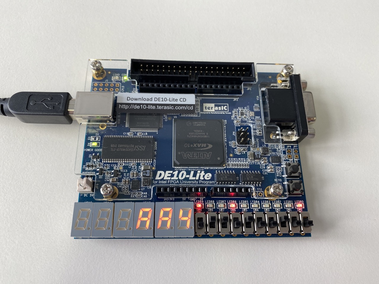
Fig. 5.5.1 Picture of the deployed arithmetic logic unit.
Shown is the configuration for inputs i_a[3:0]=4'b0100, i_b[3:0]=4'b1010 and i_alu_ctrl[1:0]=2'b01.
Let’s also use our NZCV-extended ALU alu_nzcv to program the FPGA of a DE10-Lite board.
An example configuration of the programmed board is shown in Fig. 5.5.1.
Once again we require a top-level module.
This time we use the name alu_nzcv_de10_lite and the template given in Listing 5.5.1.
Pretty much everything works analogously to the corresponding top-level module of Section 5.2.
From a high level perspective the main difference between the modules alu and alu_nzcv lies in the outputs:
alu sets the carry-out signal o_carry_out while alu_nzcv sets the condition flags o_nzcv[3:0].
Thus, in the module alu_nzcv_de10_lite we wire the NZCV flags to LEDR9 (Negative), LEDR8 (Zero), LEDR7 (Carry) and LEDR6 (oVerflow).
 1/**
 2 * Top-level module of the extended alu with condition flags.
 3 * The alu operates on the 4-bit binary numbers in SW[3:0] and SW[7:4].
 4 * The two input numbers are shown on displays HEX0 and HEX1.
 5 * The control signal is shown using LEDR1 and LEDR0.
 6 * The result is shown on display HEX2.
 7 * The NZCV flags are shown on the leds LEDR9, LEDR8, LEDR7 and LEDR6.
 8 *
 9 * @param SW bits of ten switch buttons SW9 - SW0.
10 * @param LEDR output bits corresponding to the board's ten leds LEDR9 - LEDR0.
11 * @param HEX0 output bits which drive the seven-segment display HEX0.
12 * @param HEX1 output bits which drive the seven-segment display HEX1.
13 * @param HEX2 output bits which drive the seven-segment display HEX2.
14 **/
15module alu_nzcv_de10_lite( input  logic [9:0] SW,
16                           output logic [9:0] LEDR,
17                           output logic [6:0] HEX0,
18                           output logic [6:0] HEX1,
19                           output logic [6:0] HEX2 );
20  // TODO: finished the implementation
21endmodule
Tasks
Implement the top-level module
alu_nzcv_de10_lite. Use the template in Listing 5.5.1.Compile your finished ALU in Quartus Prime and program the FPGA of a DE10-Lite board.
Make sure that the board shows the correct results for the inputs in Table 5.4.2. Provide a picture of the board for each of the inputs.