4. Field Programmable Gate Arrays
It’s time to get our hands on some actual hardware 📟 and put our new logic-design skills to the test. Most hardware components we use day-to-day have a fixed design. This means the gates and their wiring are hardwired. In other words, the design and purpose of such a device remain the same throughout its operating life. For example, suppose you buy a processor. This could be the Broadcom BCM2712 used in the Raspberry Pi 5 which we’ll use as our development platform when we discuss the Arm architecture. We can use this processor by running our software on it. Software consists of instructions that the processor executes. However, we cannot change the design of the processor itself.
In contrast, field-programmable gate arrays (FPGAs) allow us to (re)configure or “program” the logic fabric itself. This means that we can decide which logic gates to use and how they should be connected. The same manufactured FPGA could, for example, implement a tailored microprocessor one day and act as a graphics processing unit the next. In fact, FPGAs are often used as a primary platform for prototyping processor designs. For example, the RISC-V Exchange lists entire CPU-core IP blocks, including open-source options.
In this section we’ll use the DE10-Lite board, which is built around the Altera MAX 10 FPGA. Additional information beyond class time is available through FPGAcademy. We will use Quartus Prime Lite to configure the board.
Hint
Compile all your modules with Icarus Verilog using flags -Wall -Winfloop -g2012 before programming an FPGA.
Additionally, write testbenches and run simulations before opening Quartus Prime Lite.
4.1. RTL Modeling
In Section 3 we specified our hardware modules with elementary logic gates. Given an abstract description of a function, we had to manually lower it to logic gates. This process is cumbersome, error-prone and time-consuming, especially when aiming for an optimized circuit that may have multiple viable realizations. From now on, we’ll harness more powerful SystemVerilog constructs under the umbrella of register-transfer-level (RTL) modeling. This lets us write more abstract code and use a synthesis tool to generate the gate-level netlist. Even though RTL modeling greatly simplifies our work, we should keep in mind the gate-level results that synthesis will produce.
We discuss RTL modeling in class. All details can be found in the IEEE Standard for SystemVerilog. Further, Ch. 4 of the SystemVerilog Guide from Harvard’s CS141 course provides a gentler introduction.
4.2. 7-Segment Display Decoder
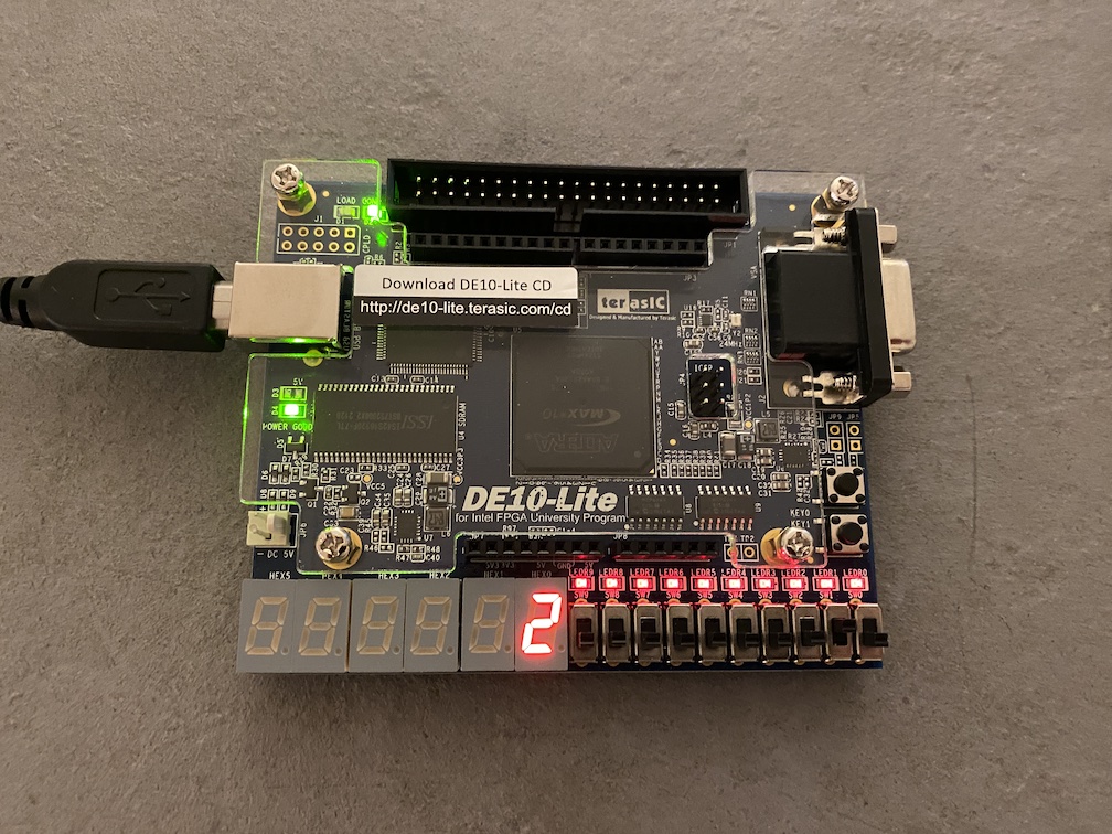
Fig. 4.2.1 Picture of the finished 7-segment display decoder where only switch SW1 is active.
The decoder connects the switches SW3, SW2, SW1 and SW0 with the display HEX0.
Thus, 0010 is the visualized binary number which corresponds to the shown hex number 2.
Let’s start our FPGA journey by designing a decoder that connects some of the board’s switches to a hexadecimal display.
For this we’ll use the first four switches SW3, SW2, SW1, and SW0.
Each switch can either be 0 (down) or 1 (up).
We may represent a hexadecimal number alternatively through exactly four binary digits.
Thus, in our design, the configuration of the four switches will encode a single hexadecimal number.
Each hexadecimal display contains seven segments.
While the DE10-Lite board has six of these displays, we’ll only use the right-most one, i.e. HEX0, in this task.
The segments of the display are active low.
Drive a segment high (1) to turn it off, low (0) to turn it on.

Fig. 4.2.2 Illustration of the hexadecimal digits 0-F when shown on a seven-segment display of the DE10-Lite board. The numbers show segment indices.
Fig. 4.2.2 illustrates all sixteen outputs our decoder might have.
For example, for the hex digit 0 all but segment 6 have to be active.
This means that we have to set all but the seventh bit of HEX0 to 0, i.e. set HEX0[6:0] to 7'b100_0000.
If we’d like to encode the hex digit 1, we’d set all bits to 1 except the second and third bits, i.e. set HEX0[6:0] to 7'b111_1001.
The respective (incomplete) truth table for our decoder is given in Table 4.2.1.
Hex Number |
SW[3:0] |
HEX0[6:0] |
|---|---|---|
0 |
|
|
1 |
|
|
2 |
|
|
3 |
|
|
4 |
|
|
5 |
|
|
6 |
|
|
7 |
|
|
8 |
|
|
9 |
|
|
A |
|
|
B |
|
|
C |
|
|
D |
|
|
E |
|
|
F |
|
|
Once again, to kickstart your work, templates for your modules are provided.
The template for the decoder module is located in Listing 4.2.1.
This template only provides the decoding cases for the two binary numbers \(0000_2\) and \(0001_2\).
The remaining 14 numbers shown in Table 4.2.1 have to be added still.
 1/**
 2 * Decoder for a seven-segment display.
 3 *
 4 * @param i_binary_number input binary number.
 5 * @param o_display output bits driving the seven-segment display.
 6 **/
 7module decoder( input  logic [3:0] i_binary_number,
 8                output logic [6:0] o_display );
 9  always_comb
10  begin
11    case( i_binary_number )
12      4'b0000: o_display[6:0] = 7'b100_0000; // 0
13      4'b0001: o_display[6:0] = 7'b111_1001; // 1
14      // TODO: add remaining hex digits 2-F
15      default: o_display[6:0] = 7'bxxx_xxxx;
16    endcase
17  end
18endmodule
Listing 4.2.2 provides a template for the top-level module.
The top-level module simply wraps our decoder.
Most importantly, we name decoder_de10_lite’s input SW and the output HEX0.
This naming scheme allows Quartus Prime Lite to recognize that SW should be the input of the first four switches and HEX0 the first hex display.
Note
Additional signal names are available from the DE10-Lite User Manual.
For example, the fifth LED is LEDR4.
We could also use Quartus Prime Lite’s pin assignment to assign the boards switches and displays to our modules’ inputs and outputs.
However, using top-level modules with respective names is simpler in the development phase.
 1/**
 2 * Top-level entry for the seven-segment display decoder.
 3 * The decoder shows the binary number represented
 4 * by SW3-SW0 of a DE10-Lite board on HEX0 as a hex number.
 5 *
 6 * @param SW bits of switches SW3, SW2, SW1 and SW0.
 7 * @param HEX0 output bits which drive the seven-segment display HEX0.
 8 **/
 9module decoder_de10_lite( input  logic [3:0] SW,
10                          output       [6:0] HEX0 );
11  // TODO: use your decoder to connect SW to HEX0
12endmodule
Tasks
Add the missing encodings for the seven-segment display to Table 4.2.1.
Implement the module
decoder. Use the template in Listing 4.2.1.Finish the implementation of the module
decoder_de10_lite. Use Listing 4.2.2’s template.Compile your modules in Quartus Prime Lite and program the FPGA of a DE10-Lite board.
Make sure that the board shows the correct hexadecimal numbers in display
HEX0for all combinations of the switchesSW0,SW1,SW2,SW3. Provide three pictures of the programmed FPGA for the hex numbers7,BandE. One should see the hex display and the switches in your pictures. An example is given in Fig. 4.2.1.
4.3. Tiny Calculator
Now that we have a way to display four-bit binary numbers, let’s take it up a notch.
In this task we’ll implement a tiny calculator that takes two four-bit binary numbers \(A_{[3:0]}\) and \(B_{[3:0]}\) as inputs.
We map the first four switches, SW[3:0], to \(A_{[3:0]}\) and the next four, SW[7:4], to \(B_{[3:0]}\).
Our tiny calculator computes the five-bit result \(C_{[4:0]} = A_{[3:0]} + B_{[3:0]}\).
We display the input \(A_{[3:0]}\) on HEX0 and \(B_{[3:0]}\) on HEX1.
The result \(C_{[4:0]}\) has five bits due to the carry-out.
Thus, we use two hex digits for \(C_{[4:0]}\).
One for the four bits [3:0] (shown on HEX2) and one for the carry-out on HEX3.
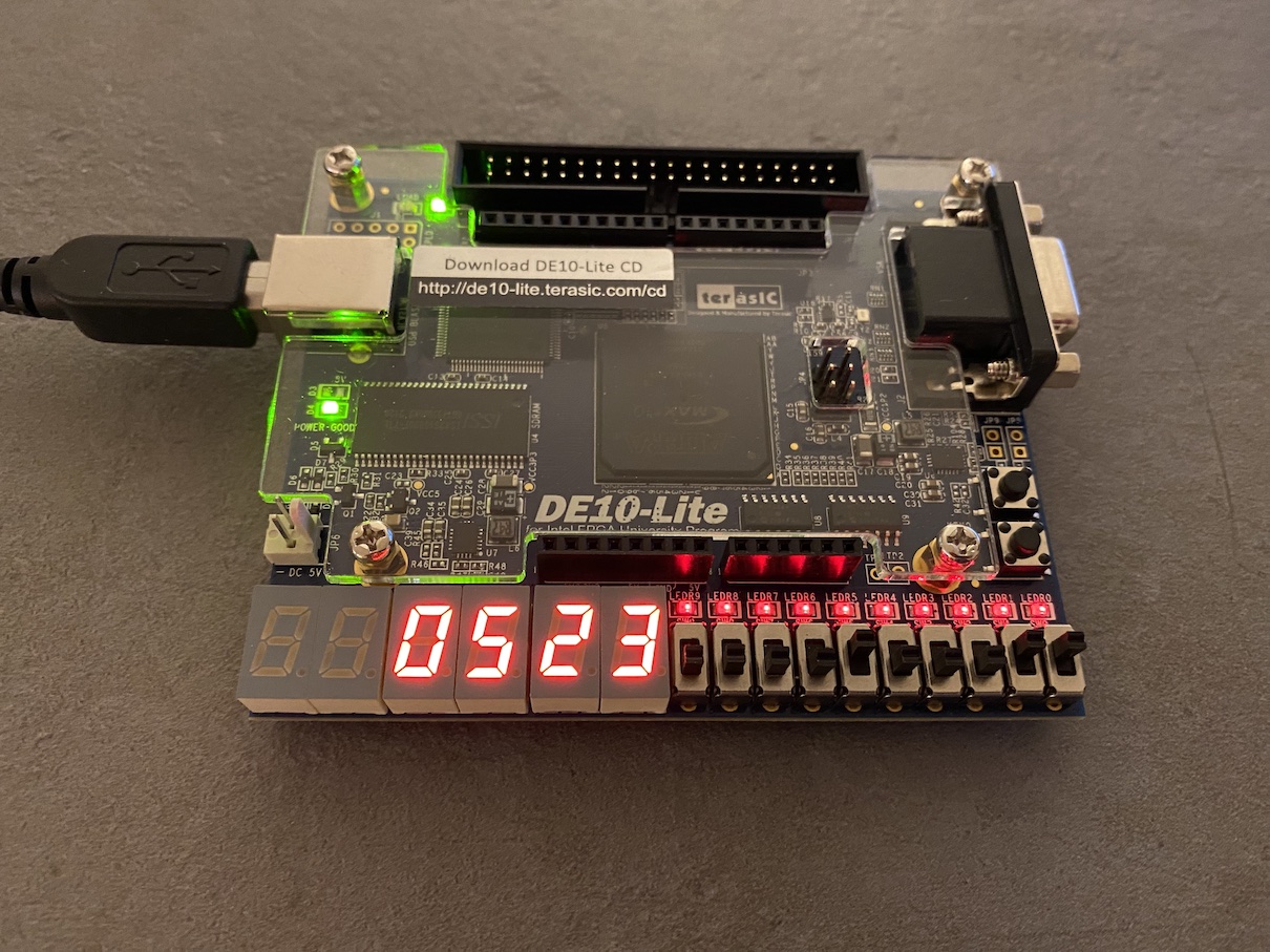
Fig. 4.3.1 Picture of the tiny calculator in action.
In the configuration shown, only switches SW0, SW1 and SW5 are up (1).
This means \(A_{[3:0]} = 0011_2\), \(B_{[3:0]} = 0010_2\) and \(C_{[4:0]} = 00101_2\).
We see that the corresponding hexadecimal representations appear on displays HEX0 - HEX3: \(0011_2 = 3_{16}\) on HEX0, \(0010_2 = 2_{16}\) on HEX1 and \(00101_2 = 05_{16}\) split across HEX2 and HEX3.
A picture of an example is provided in Fig. 4.3.1.
Here, SW[3:0] = 4'b0011 and SW[7:4] = 4'b0010.
The corresponding hexadecimal numbers \(3_{16}\) and \(2_{16}\) are shown on HEX0 and HEX1.
Additionally, HEX2 and HEX3 show the result \(05_{16}\).
SW[3:0] |
SW[7:4] |
HEX0[6:0] |
HEX1[6:0] |
HEX2[6:0] |
HEX3[6:0] |
|---|---|---|---|---|---|
|
|
|
|
|
|
|
|
|
|
|
|
|
|
|
|
|
|
|
|
|
|
|
|
|
|
|
|
|
|
 1/**
 2 * Top-level entry of the tiny calculator.
 3 * The calculator adds the 4-bit binary numbers in SW[3:0] and SW[7:4].
 4 * The two inputs are shown on displays HEX0 and HEX1.
 5 * The result of the addition is shown on displays HEX2 and HEX3.
 6 *
 7 * @param SW bits of switches SW7, SW6, SW5, SW4, SW3, SW2, SW1 and SW0.
 8 * @param HEX0 output bits which drive the seven-segment display HEX0.
 9 * @param HEX1 output bits which drive the seven-segment display HEX1.
10 * @param HEX2 output bits which drive the seven-segment display HEX2.
11 * @param HEX3 output bits which drive the seven-segment display HEX3.
12 **/
13module tiny_calculator( input  logic [7:0] SW,
14                        output logic [6:0] HEX0,
15                        output logic [6:0] HEX1,
16                        output logic [6:0] HEX2,
17                        output logic [6:0] HEX3 );
18  // TODO: implement the tiny calculator
19endmodule
Tasks
Implement the module
tiny_calculator. Use the template in Listing 4.3.1 as a basis for your module. Use your four-bit ripple carry adder of Section 3.3 for the addition.Add the testbench
tiny_calculator_tbfor yourtiny_calculatormodule. Check that your calculator produces the correct outputs, i.e. the bitsHEX0[6:0],HEX1[6:0],HEX2[6:0],HEX3[6:0]for all inputs in Table 4.3.1.Compile your module in Quartus Prime Lite and program the FPGA of a DE10-Lite board.
Make sure that the board’s displays show the correct hexadecimal numbers for the configurations in Table 4.3.1. Provide a picture for each of the five configurations.