In this experiment, we will draw and inspect our first combinational circuit using the Digital tool.
The circuit represents the simple XOR expression of two inputs and one output given by
The truth values for this expression are stated in Table 1.2.1.
Table 1.2.1 Truth-table for the XOR expression stated in Eq. (1.2.1).
A
0
0
1
1
B
0
1
0
1
Y
0
1
1
0
Tasks
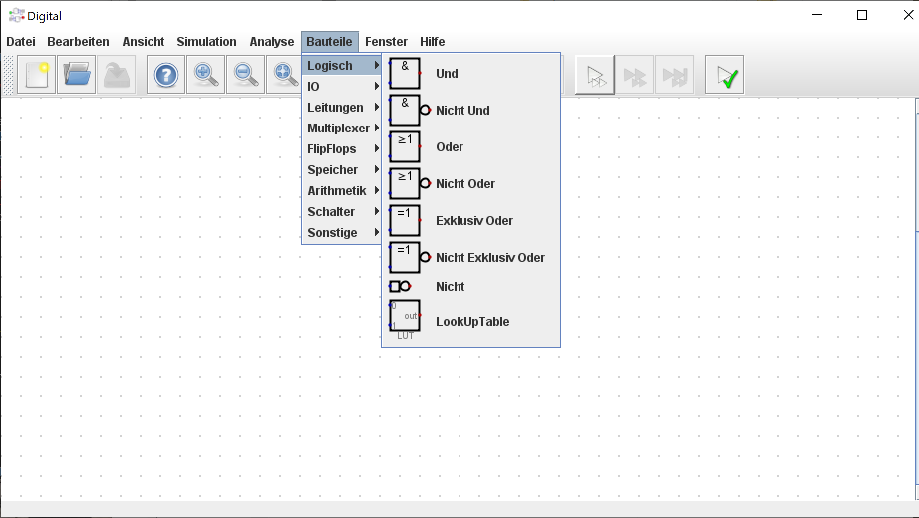
Open the Digital tool draw the circuit. Therefore, add
one XOR gate, two inputs and one output to the workspace by choosing the correct items from the menu
(Bauteile/Logisch and Bauteile/IO) - compare Fig. 1.2.1.
Fig. 1.2.1 Workspace to draw circuits and menu to add items.
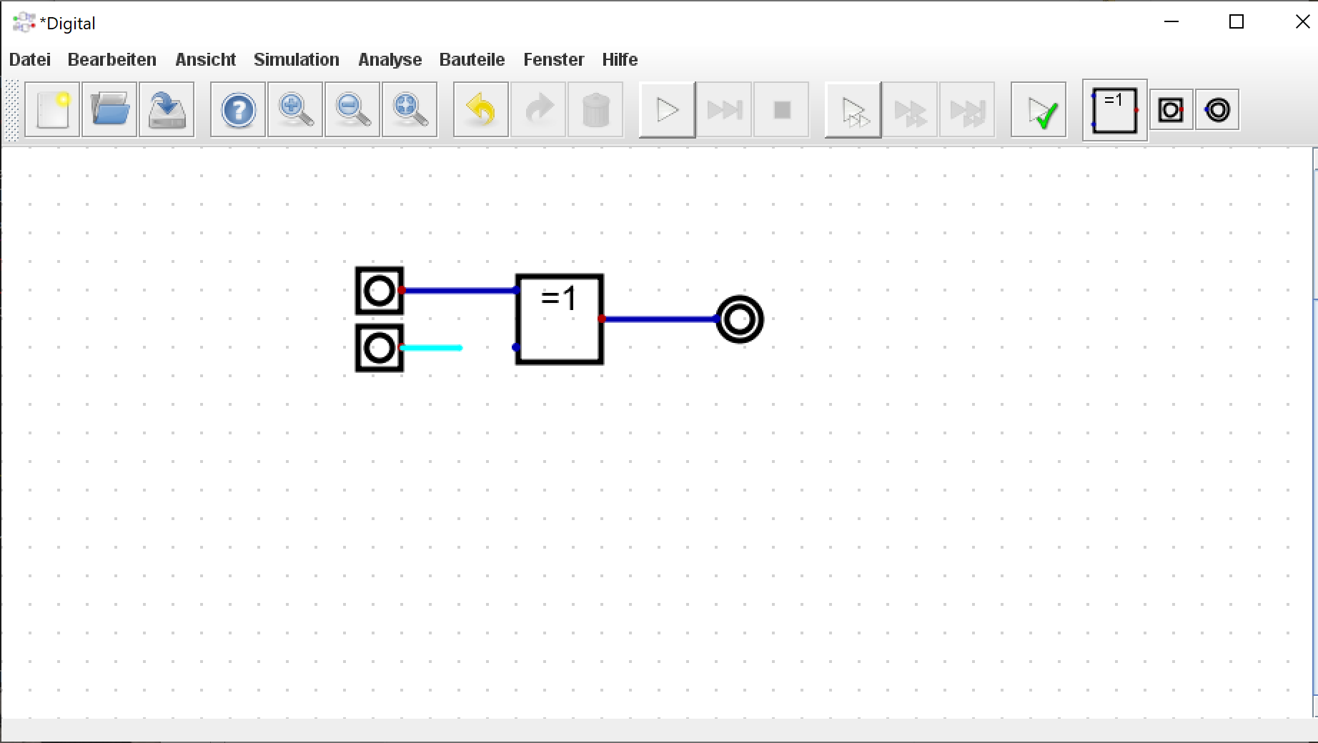
Use the mouse (left-click) to connect the XOR gate with the inputs and output - compare Fig. 1.2.2.
Fig. 1.2.2 Drawing connections between the XOR gate and the in-/outputs.
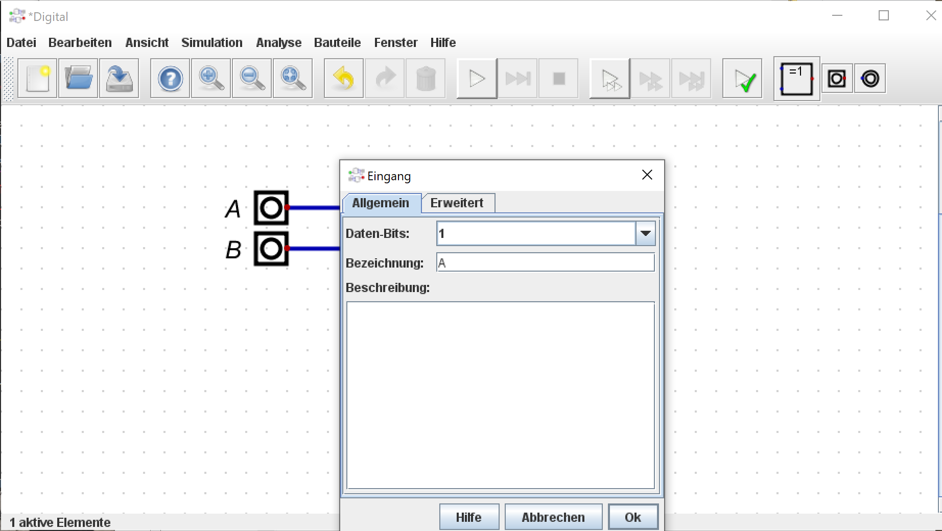
Label the inputs and outputs (right-click on the item) and insert an appropriate
name for the item - compare Fig. 1.2.3.
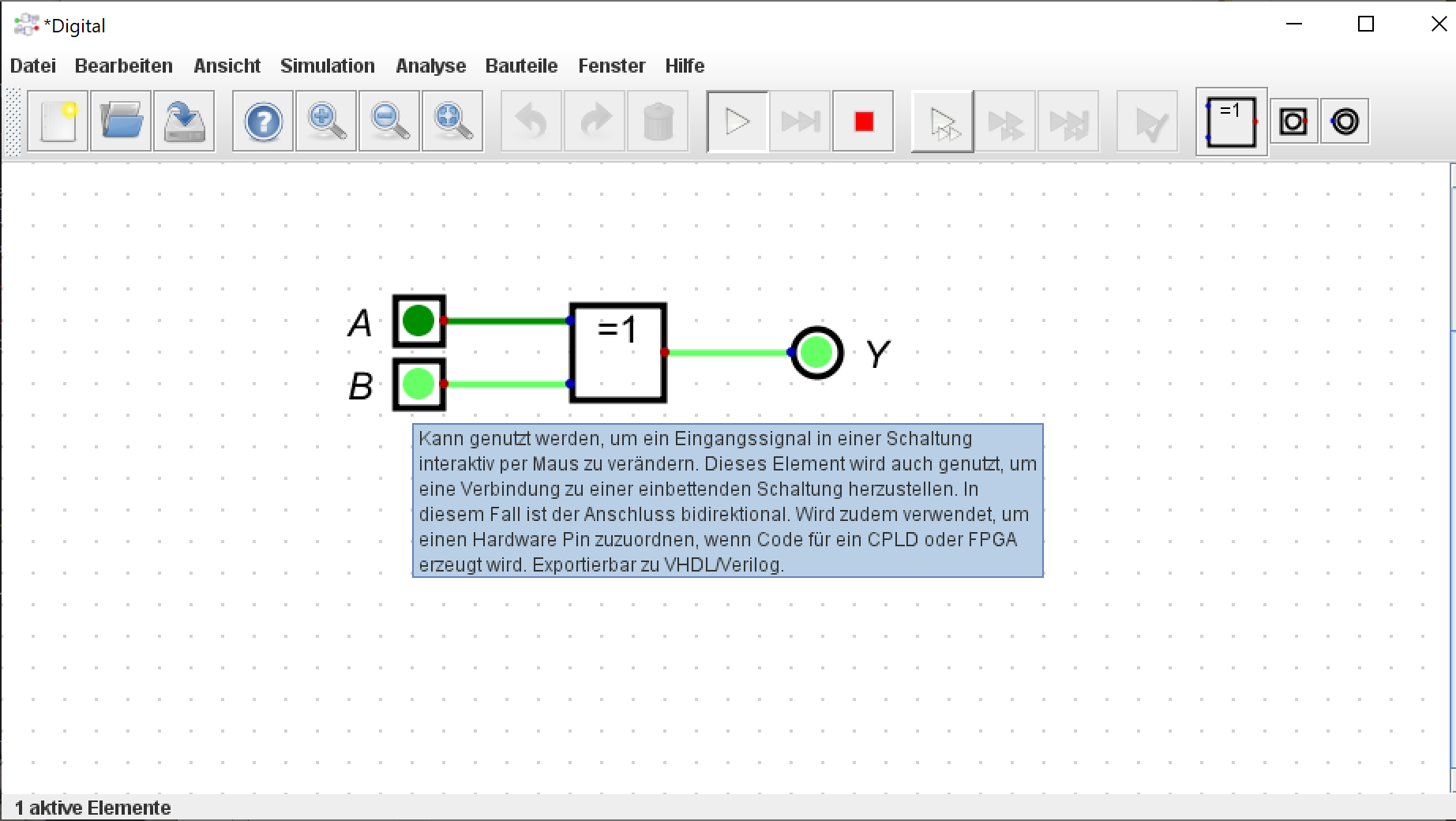
Run your circuit (press play button)
and test if it produces the correct results by activating different combinations of the inputs
- compare Fig. 1.2.4.
In this experiment, we will draw a reformulated combinational circuit using the Digital tool.
The original circuit represents the simple XOR expression of two inputs and one output
given by the XOR expression in (1.2.1) with the truth table stated in Table 1.2.1.
Tasks
Use the truth table to design a logical circuit that only consists of AND, OR, and NOT gates.
In this experiment, we will derive a logical circuit for the half adder logic shown in Fig. 1.5.1.
In contrast to the depicted circuit, the new circuit will only uses AND, OR, and NOT gates.
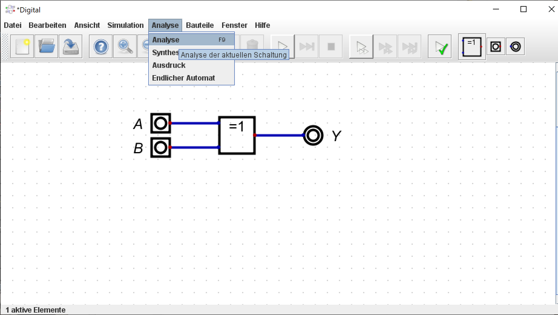
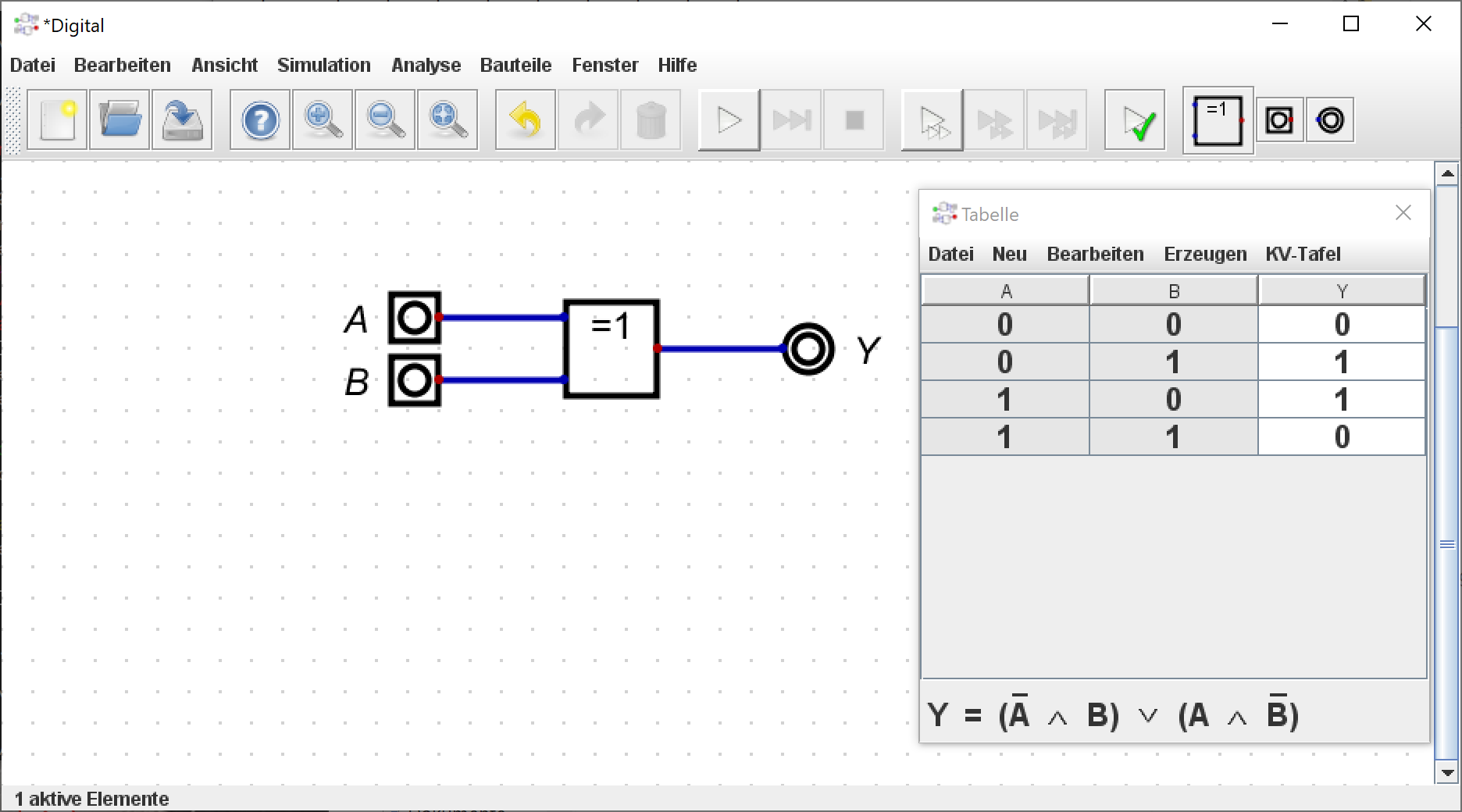
Use the analyse option to derive the truth table for the circuit.
Based on this truth table, design a new equivalent circuit that only uses AND, OR, and NOT gates.
As before, use the truth tables to validate the equivalence of both circuits.
Save and submit both circuits (as half_adder_orig.dig and half_adder_new.dig) besides
their truth tables (in csv-format as half_adder_orig.csv and half_adder_new.csv).
Use the analyse option to derive the truth table for the circuit.
Based on this truth table, design a new circuit that only uses AND, OR, and NOT gates.
As before, use the truth tables to validate the equivalence of both circuits.
Save and submit both circuits (as full_adder_orig.dig and full_adder_new.dig) besides
their truth tables (in csv-format as full_adder_orig.csv and full_adder_new.csv).
In this experiment, we will develop a combinational circuit for a 2-Bit adder that has four inputs (A1, A0, B1, B0) and three outputs (Y1, Y0, C)
with the truth values stated in Table 1.7.1.
Table 1.7.1 Truth-table for the 2-bit adder circuit to be designed.
A1
0
0
0
0
0
0
0
0
1
1
1
1
1
1
1
1
A0
0
0
0
0
1
1
1
1
0
0
0
0
1
1
1
1
B1
0
0
1
1
0
0
1
1
0
0
1
1
0
0
1
1
B0
0
1
0
1
0
1
0
1
0
1
0
1
0
1
0
1
Y1
0
0
1
1
0
1
1
0
1
1
0
0
1
0
0
1
Y0
0
1
0
1
1
0
1
0
0
1
0
1
1
0
1
0
C
0
0
0
0
0
0
0
1
0
0
1
1
0
1
1
1
Tasks
Use several copies of the full adder circuit from the previous experiment to design
the 2-bit adder circuit using the Digital tool
as indicated in the schematic
Fig. 1.7.1 2-bit adder schematic using full adder circuits.
Hint: You can select (parts of) a circuit on the workspace
(click the left mouse button, hold the mouse button, adapt selection square and then release the mouse button) and copy-paste items
using the menu (Bearbeiten/Kopieren and Bearbeiten/Einfügen) or keyboard short-cuts (CTRL-C and CTRL-V).
Use the analyse option to derive the truth table for your designed circuit and validate its correcntess.
Save and submit the circuit (as 2bit_adder.dig) besides
its truth table (in csv-format as 2bit_adder.csv).