In contrast to combinational logic design, sequential logic design does not only depend on current inputs
but but also on prior inputs. The information stored within a circuit are often called state variables.
In this section, we will consider some simple circuits like latches and flip-flops that allow to store state variables
and are the building blocks for more complex synchrounous sequential logic circuits.
It consists of two cross coupled NOR gates and allows to store and control one bit of information as a state variable.
as indicated by the truth values in Table 3.1.1.
Table 3.1.1 Truth-table for the SR-Latch circuit depicted in Fig. 3.1.1.
0
0
1
1
0
1
0
1
0
1
0
1
0
0
In this experiment, we will use the Digital tool to investigate its behavior by examining its wavefront.
Tasks
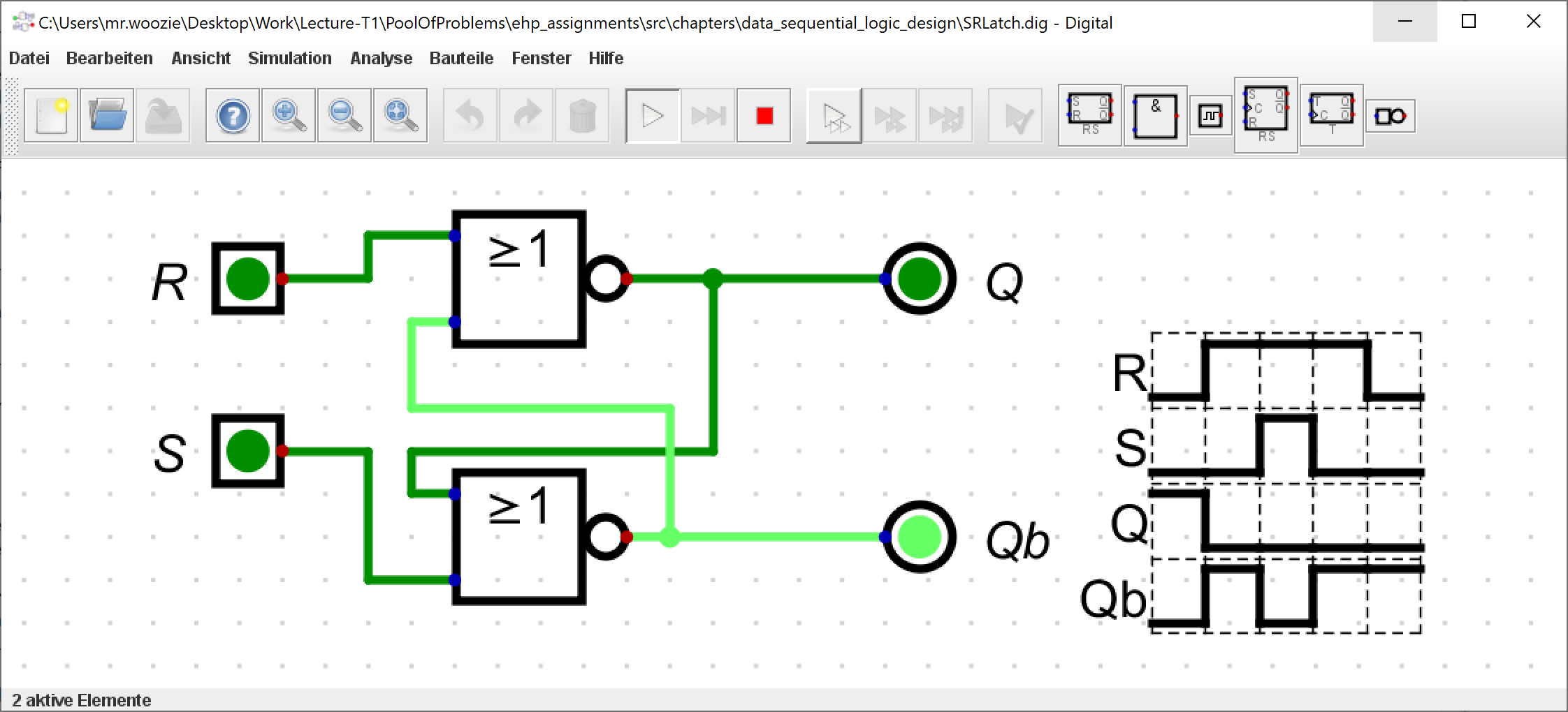
Use the Digital tool to draw the SR-Latch Circuit shown in Fig. 3.1.1
Add appropriate labels to the inputs and outputs of the circuit.
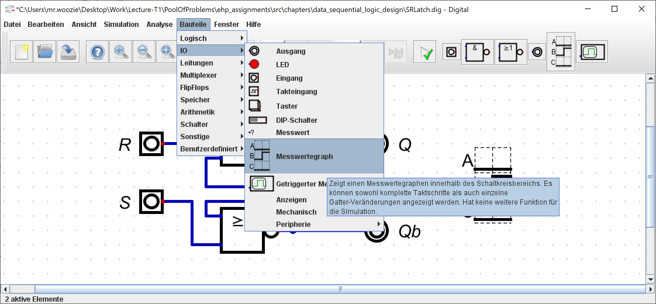
Add a wavefront (Bauteile/IO/Messwertegraph) to the drawing.
Run your circuit and examine the wavefront for various combinations of inputs.
Fig. 3.1.3 Wavefront for a running SR-Latch circuit.
Validated that it produces the correct output as stated in Table 3.1.1.
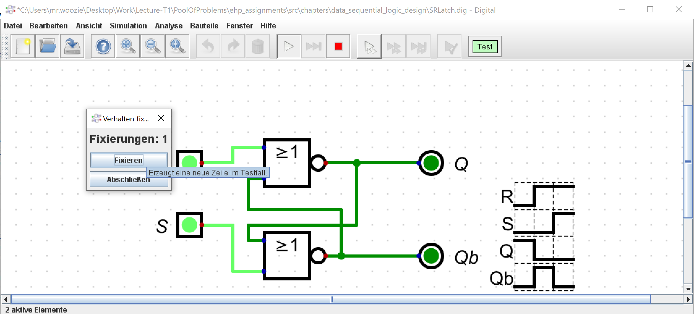
In the menu (Bearbeiten/Verhalten fixierenden Testfall erstellen), you will also find the option to specify certain test cases.
Use this option to fix various different inputs to test the behaviour of the circuit.
Fig. 3.1.4 Creating test cases by fixing a combination of different inputs.
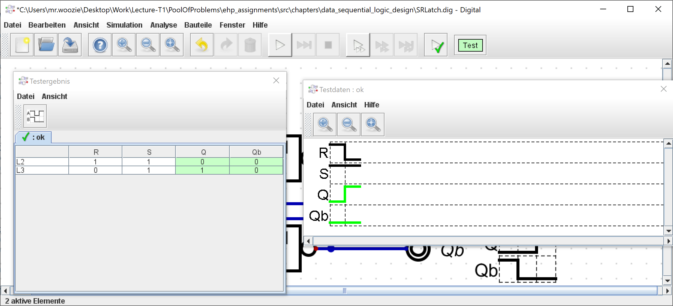
Once you are done with fixing suitable inputs, you can run the test case and examine the resulting truth table and wavefront.
Hint
Press the play button with the green check symbol.
Fig. 3.1.5 Resulting wavefront and truth table for a test case with different fixed inputs.
Save and submit all important information, namely, the circuit (as SR-latch.dig), the truth table (as SR-latch.csv), and
the wave front (as SR-latch.svg).
Note that the inputs and
of the SR-Latch are used to reset (if ), to set (if ) or to output (if ) the previous value of the state variable at .
In this experiment, we will examine an extension of the SR-Latch circuit called D-Latch.
Similar to the SR-Latch, the D-Latch circuit has two inputs ( and ) and two outputs ( and ) as depicted in Fig. 3.2.1.
In contrast to the SR-Latch, the input of the D-Latch now controls when the state should change and the input acts as a data input determining what the next state variable shall be - compare Table 3.2.1.
Table 3.2.1 Truth-table for the D-Latch circuit depicted in Fig. 3.2.1.
0
1
1
0
1
0
1
1
0
Tasks
Use the Digital tool to draw the D-Latch Circuit using the SR-Latch from the previous experiment
as depicted in Fig. 3.2.1.
Add appropriate labels to the inputs and outputs of the circuit besides a wavefront to the circuit.
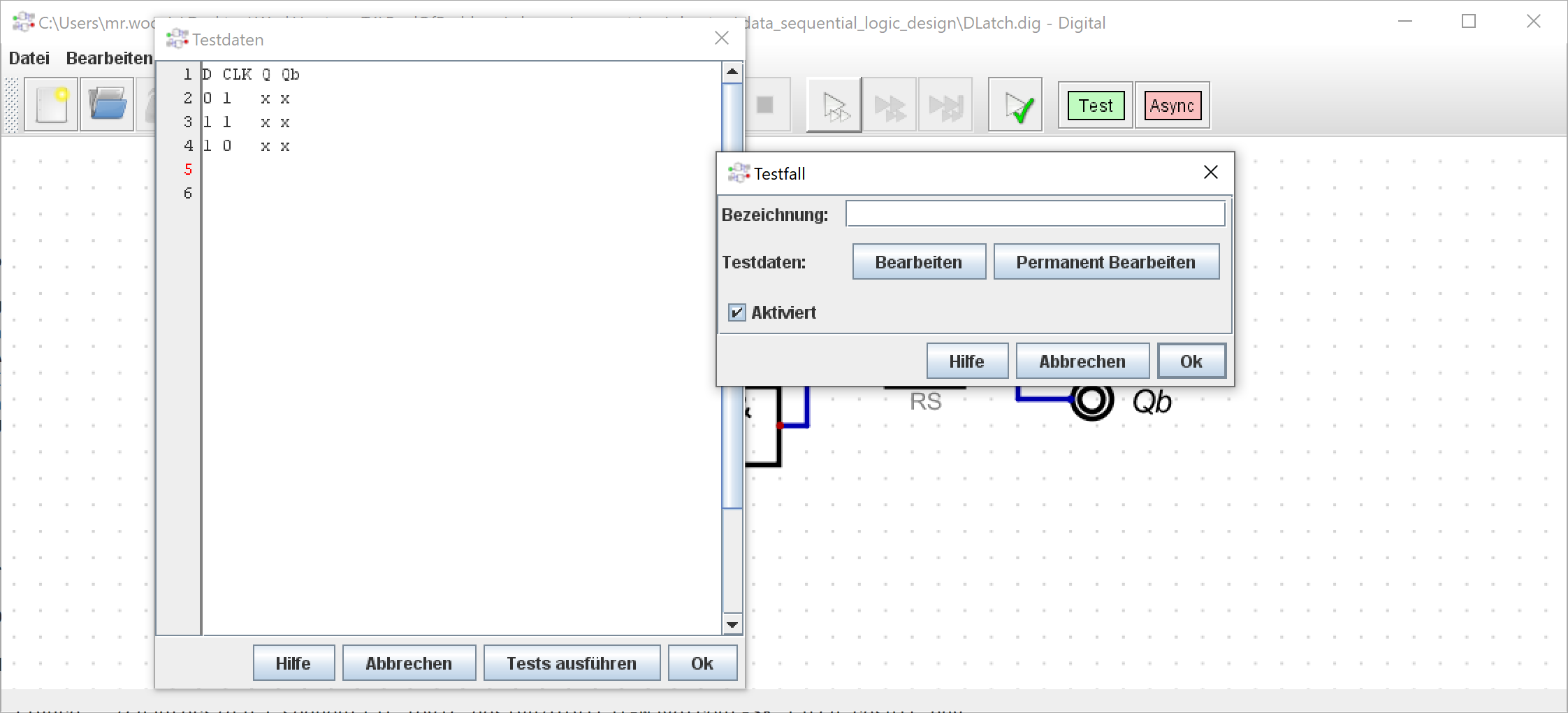
In contrast to the previous experiment, we will now add an test environment (Bauteile/Sonstige/Testfall) to the circuit.
This allows to encode different input settings for evaluating the circuit and validating its correctness
(right click on the green Test item and press on PermanentBearbeiten).
Fig. 3.2.2 Creating a test environment for a circuit.
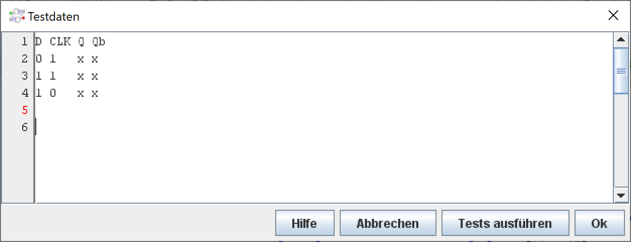
As shown in Fig. 3.2.3,
the different settings for each labeled item of the circuit are encoded (columnwise) in the text field.
Here, the first row is used to assign each column to a specific circuit item.
The following rows describe the different values to be tested for each item in a step, where
1/0 correspond to true/false and x represents an undefined value.
Hint
Use undefined values X if you are not sure what an output will be.
Fig. 3.2.3 Encoding a combination of different inputs in the test environment.
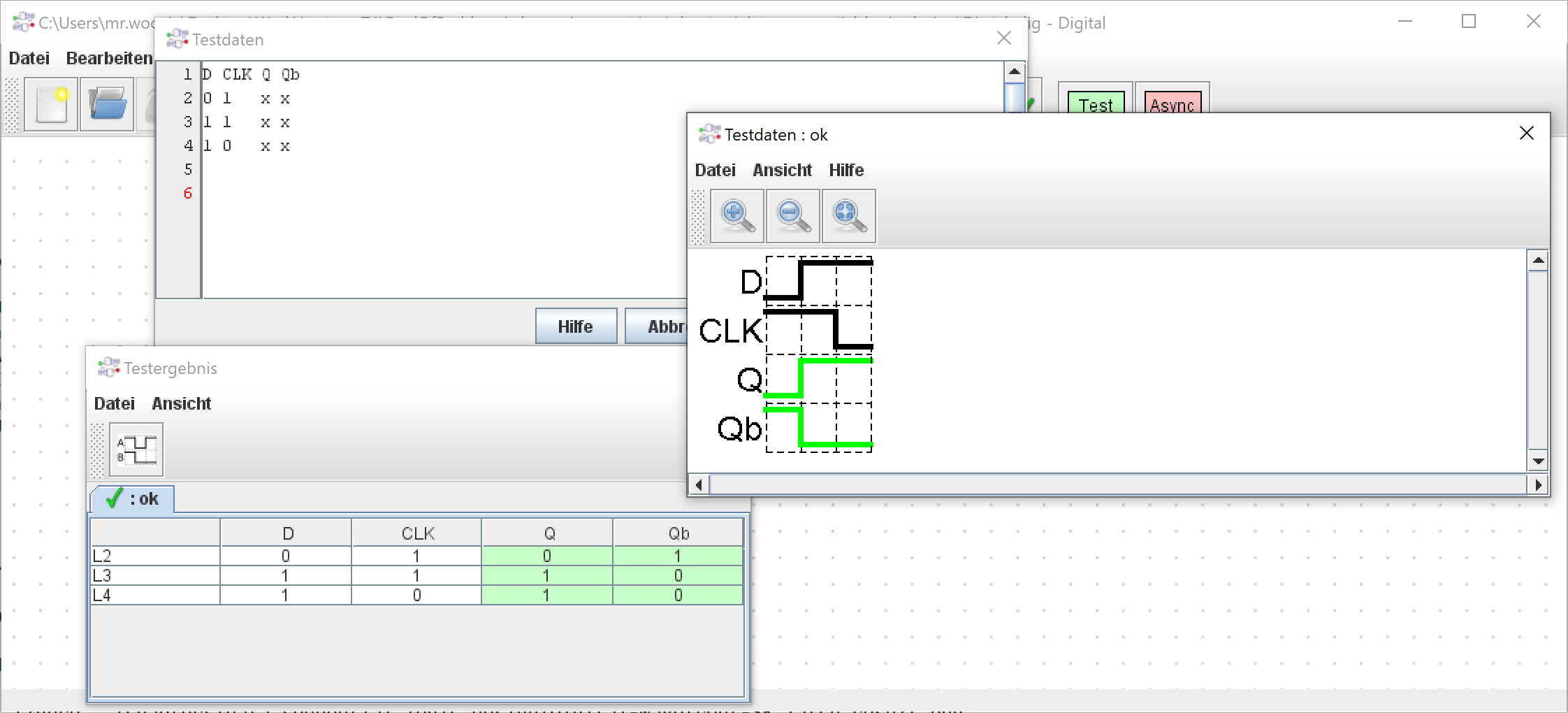
Once you are done with encoding the test environment, you can run the test case (Tests ausführen) and examine the resulting truth table and wavefront.
Fig. 3.2.4 Results of the test and corresponging waveform of the test environment.
Save and submit all important information, namely, the circuit (as D-latch.dig), the test file with your encoding (as D-latch.txt), the test result (as D-latch.csv) and the wave front (as D-latch.svg).
As a last example, we will examine D-Flipflop circuits as depicted in Fig. 3.3.1.
They are almost identical to the D-Latches from the previous experiment but are edge-triggered.
Namely, the D-Latch is transparent when the control bit is set, i.e., , whereas the D-Flipflop circuit
copies the value of the data input to the output on the rising edge of .
To see this effect, we will compare the wavefront of the sequential D-Latch circuit and the D-Flipflop circuit to see this difference.
Draw the D-Flipflop circuit using the D-Latch circuits from the previous experiment as shown in Fig. 3.3.1.
Add a seperate D-Latch circuit to your drawing
and connect both circuits (D-Flipflop and D-Latch) to the same inputs ( and ).
Add appropriate labels to the seperate outputs of the two circuits, for example, and .
Use the test environment with the following inputs to show the difference between both circuits.
Hint
Assign undefined values to the outputs.
Fig. 3.3.2 Wavefront for the inputs:math:CLK and .
Save and submit all important information, namely, the circuits (as D-Latch_vs_D-Flipflop.dig),
the truth table (as D-Latch_vs_D-Flipflop.csv), and the wave front (as D-Latch_vs_D-Flipflop.svg).


 and
and  of the SR-Latch are used to reset (if
  ), to set (if
  ) or to output (if
  ) the previous value of the state variable at
  .
. and
and  ) and two outputs (
 ) as depicted in Fig. 3.2.1.

 , whereas the D-Flipflop circuit
copies the value of the data input
, whereas the D-Flipflop circuit
copies the value of the data input 
 and
and  .
.